
CASE STUDIES
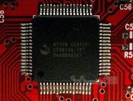 With error correcting code synchronization SRAM, effectively release the P
Ultra small volume CAN CANFD isolation transceiver module of TD - MCAN TD - MCANFD series Integrated power supply isolation, signal isolation, the CAN transceiver and bus protection in the integr
Show Detail >>
 Nonvolatile memory is a good opportunity
In recent years the Internet development in full swing, the boom will push memory requirements Cars, mobile device, industrial device such as a machine to machine (M2M) several years of rising demand for solid-state drives, combined with embedded system w
Show Detail >>
 Semiconductor giant developing eMRAM memory
In addition to the high speed computing and data center storage requirements, non-volatile memory, the Internet of things need instant information storage requirements, involving the Internet of things need data high durability, low energy consumption, ev
Show Detail >>
 Storage solutions - external SRAM based on FPGA
externalSRAMRefers to the connection in the FPGA external static RAM (SRAM) There are many kinds of external SRAM memory also For the choice of external SRAM is decided by the nature of the application requirements Both advantages and disadvantages of usi
Show Detail >>
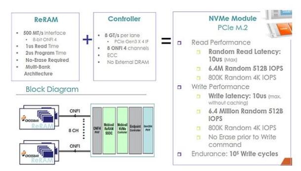 Based on the technology of ReRAM SSD forthcoming
SSD though can be stacked layers to increase the single grain capacity, but as the layer number increasing, the number, the more need of silicon perforation manufacturing difficulty increase, not only the production cost is high, the roa also cannot be gu
Show Detail >>
 SRAM will disappear?
After decades of development and progress, the electronics industry almost formed a linear system, and by Moore s Law (Moore s Law) However, as Moore s law has gradually become loose, many new technologies gradually began to float on the table The
Show Detail >>
 Three large capacity, high speed nonvolatile SRAM contrast
In embedded systems, the use most non-volatile memory block is the EEPROM and FLASH (Non - Volatile), is mainly used to save the program or data, but the two have a common memory defect is slow to write, write algorithm is more complex, and cannot meet th
Show Detail >>
 Introducing Bluetooth mesh networking
Bluetooth mesh capability enables many-to-many device communications in large-scale device networks for building automation sensor networks and other IoT solutions
Show Detail >>CONTACT US
Zarchin 10St.Raanana,43662 Israel
238884 Singapore