THREE-LEVEL FLASH GIVES WAY TO FOUR IN BID FOR GREATER CAPACITY
Flash memory has been a disruptive technology from its industrial inception in the early '90s and innovation is still ongoing after more than 25 years. Today the most advanced storage products use NAND flash. Thanks to its storage density, quality and reliability NAND has changed our lives. Through continuous development, investments and improvements by flash vendors such as Toshiba and Intel, the technology has become a mainstream consumer product as well as a robust and reliable solution for embedded applications.
The influence of market demand and advancements in manufacturing resulted in 2D NAND reaching its highest point of technological maturity. On the one hand, 2D SLC NAND offers extremely fast access times, low latencies, good energy efficiency and robustness. However, from an economical perspective investing into the production of 2D NAND is not financially viable for vendors anymore, given the demands for larger capacities. Each successive shrink of the cells enabled manufacturers to produce a higher cell count per wafer. Starting out with a cell size of 350nm in 1997 vendors are now able to produce 2D NAND flash cells with a 16nm structure. This in turn led to lower prices for 2D NAND flash and better availability due to a higher GB per wafer yield.
However, the miniaturisation of NAND flash also brought along several technical limitations to flash vendors. One major limitation is that with each shrinking process of the cells the number of available electrons becomes substantially less.
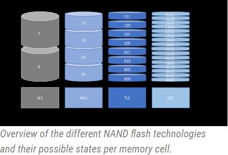
For example, the number of electrons in a flash cell with a lithography of 16nm is around ≤20. A multi-level-cell (MLC) NAND flash has four fixed voltage levels. Each fixed voltage level represents one of the following binary codes: 00, 01, 10, 11. With each successive program and erase cycle the risk of electrons being trapped between the substrate and control gate increases. The more electrons are trapped the higher the chance of voltage levels not being correctly read out by the controller. Without complex controller and firmware features, such as error correction code, the data on the NAND flash would be corrupt and unusable. In the worst case, if the NAND flash contained essential booting data for the operating system, the system put simply, 2D NAND flash has reached its physical limitations. Any further shrinking would undermine the reliability, endurance and data retention of the NAND flash.
From an economical perspective, the market requires storage devices with higher capacities and better performance as our world is becoming more data-centric. Estimations project that an average connected person will interact with smart devices nearly 4800 times per day and that by 2025 163 ZB of data will be created on an annual basis. The unprecedented growth of smart devices in combination with artificial intelligence requires hardware that is capable of handling more storage, processing and analysing of data.
Vendors have taken two major steps to fulfil the markets requirement for larger capacities at an affordable price while at the same time delivering high reliability, uncompromised data integrity and consistent performance. The first method by vendors to increase storage density was the introduction of a third NAND dimension: multilevel storage. The first NAND flash memories only had a single-level cell (SLC) architecture, and were therefore only capable of storing one bit per memory cell. This was followed by the multi-level cell (MLC) and the triple-level cell (TLC) architectures, which can store two or three bits, respectively. In the MLC, four voltage levels are used to represent the four possible combinations of two binary digits, while the readout circuitry of a TLC has to reliably distinguish between eight discrete voltage levels to capture the three bits of stored data.
The second and more revolutionary method by vendors was to move from the traditional planar NAND structure to a three-dimensional architecture. This architecture is capable of higher areal density in comparison to 2D NAND and provides room for scalability in the future. Just like a skyscraper can shelter more people in comparison to a single storey house, so too can a 3D-NAND flash cell store more data than a 2D flash cell. By having better areal density, vendors can scale to larger capacities by delivering more gigabytes per wafer. This technological leap allows vendors to already produce SSD drives that can go all the way up to 64 TB. Regarding reliability and quality, the BiCs3 NAND flash from Toshiba delivers the same amount of program and erase cycles in comparison to the Toshiba 15nm 2D MLC. However, the price to performance ratio is the key advantage of the technology.
Such three-dimensional NAND (3D NAND) flash memories have therefore taken what was a linear ‘string’ of flash cells making up a word line in a 2D memory array and, conceptually speaking, folded them up into the third dimension in form of a U shape, with each cell being defined by alternating layers of material. The more discrete layers of material that can be laid down by the manufacturing process, the more discrete flash cells can be built in the same die area. Hence the greater the device’s overall capacity.
The influence of market demand and advancements in manufacturing resulted in 2D NAND reaching its highest point of technological maturity. On the one hand, 2D SLC NAND offers extremely fast access times, low latencies, good energy efficiency and robustness. However, from an economical perspective investing into the production of 2D NAND is not financially viable for vendors anymore, given the demands for larger capacities. Each successive shrink of the cells enabled manufacturers to produce a higher cell count per wafer. Starting out with a cell size of 350nm in 1997 vendors are now able to produce 2D NAND flash cells with a 16nm structure. This in turn led to lower prices for 2D NAND flash and better availability due to a higher GB per wafer yield.
However, the miniaturisation of NAND flash also brought along several technical limitations to flash vendors. One major limitation is that with each shrinking process of the cells the number of available electrons becomes substantially less.
For example, the number of electrons in a flash cell with a lithography of 16nm is around ≤20. A multi-level-cell (MLC) NAND flash has four fixed voltage levels. Each fixed voltage level represents one of the following binary codes: 00, 01, 10, 11. With each successive program and erase cycle the risk of electrons being trapped between the substrate and control gate increases. The more electrons are trapped the higher the chance of voltage levels not being correctly read out by the controller. Without complex controller and firmware features, such as error correction code, the data on the NAND flash would be corrupt and unusable. In the worst case, if the NAND flash contained essential booting data for the operating system, the system put simply, 2D NAND flash has reached its physical limitations. Any further shrinking would undermine the reliability, endurance and data retention of the NAND flash.
From an economical perspective, the market requires storage devices with higher capacities and better performance as our world is becoming more data-centric. Estimations project that an average connected person will interact with smart devices nearly 4800 times per day and that by 2025 163 ZB of data will be created on an annual basis. The unprecedented growth of smart devices in combination with artificial intelligence requires hardware that is capable of handling more storage, processing and analysing of data.
Vendors have taken two major steps to fulfil the markets requirement for larger capacities at an affordable price while at the same time delivering high reliability, uncompromised data integrity and consistent performance.

The second and more revolutionary method by vendors was to move from the traditional planar NAND structure to a three-dimensional architecture. This architecture is capable of higher areal density in comparison to 2D NAND and provides room for scalability in the future. Just like a skyscraper can shelter more people in comparison to a single storey house, so too can a 3D-NAND flash cell store more data than a 2D flash cell. By having better areal density, vendors can scale to larger capacities by delivering more gigabytes per wafer. This technological leap allows vendors to already produce SSD drives that can go all the way up to 64 TB. Regarding reliability and quality, the BiCs3 NAND flash from Toshiba delivers the same amount of program and erase cycles in comparison to the Toshiba 15nm 2D MLC. However, the price to performance ratio is the key advantage of the technology.
Such three-dimensional NAND (3D NAND) flash memories have therefore taken what was a linear ‘string’ of flash cells making up a word line in a 2D memory array and, conceptually speaking, folded them up into the third dimension in form of a U shape, with each cell being defined by alternating layers of material. The more discrete layers of material that can be laid down by the manufacturing process, the more discrete flash cells can be built in the same die area. Hence the greater the device’s overall capacity.
CONTACT US
USA
Vilsion Technology Inc.
36S 18th AVE Suite A,Brington,Colorado 80601,
United States
E-mail:sales@vilsion.com
Europe
Memeler Strasse 30 Haan,D 42781Germany
E-mail:sales@vilsion.com
Middle Eastern
Zarchin 10St.Raanana,43662 Israel
Zarchin 10St.Raanana,43662 Israel
E-mail:peter@vilsion.com
African
65 Oude Kaap, Estates Cnr, Elm & Poplar Streets
Dowerglen,1609 South Africa
E-mail:amy@vilsion.com
Asian
583 Orchard Road, #19-01 Forum,Singapore,
238884 Singapore
238884 Singapore
E-mail:steven@vilsion.com
