Monolithic 3D: Promise, Challenges
Researchers said monolithic 3D chip stacks have promise but face several challenges at an event attended by CEA-Leti, Qualcomm, ARM and others.

Leti and others point to exiting CMOS image sensors from Sony as a first example of commercial silicon using M3D techniques to link logic and memory. In January, Sony presented a paper on a three-layer stack with help from Samsung. For its part, Samsung said recently it will put peripheral circuits on a future 3D NAND chip, suggesting an M3D-like approach.


BURLINGAME, Calif. — Monolithic 3D integration shows promise as a way to create faster, cheaper, smaller chips. But despite interest from several quarters, most efforts are still in a research stage with significant work ahead in proving the technology and building an ecosystem for it.
That was the take away from the annual S3S conference here where ARM, CEA-Leti, DARPA, Mentor Graphics and Qualcomm presented work in the field. M3D aims to carve diverse functions into blocks stacked vertically in one or more die, however most approaches have not yet demonstrated commercial viability.
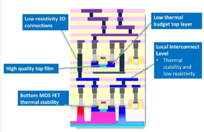
The Leti European research insitute has worked for several years on Cool Cube, an approach for vertically stacking transistors. IBM, Qualcomm and STMicroelectronics are among Leti’s partners on the project. While it holds promise, it has yet to show how it can scale to problems such as global routing in a full M3D chip.
A Qualcomm research director co-hosted a half-day program on Cool Cube here. His enthusiasm for the area which he named 3D VLSI was clear, as was the vigor with which he is still exploring many shortcomings of current approaches.
Years ago, Qualcomm was equally vigorous exploring through silicon vias (TSVs), an approach many thought would be used for mobile application processors. But today, Qualcomm has largely dropped that effort because the thermal and cost challenges for TSVs in such chips remain largely unsolved. Meanwhile TSMC and others have made advances in wafer-level fan-out packaging now used in Apple’s iPhone processors
Startup MonolithIC3D has been championing M3D with its CEO, semiconductor veteran Zvi Or-Bach, acting as an organizer for the event. The five-person company with Or-Bach as its only full-time employee is said to have compelling ideas and IP for M3D, but it has yet to find a partner to test them in silicon.
DARPA sees M3D as one of many promising efforts to reinvigorate the chip industry at a time when it is seeing slowing gains and rising costs. One of six DARPA programs on next-generation silicon design will explore chip stacks, and some companies have said they will proposed M3D projects for it.
Top challenges for M3Ds include:
Getting EDA giants to build design tools for it
Protecting components from high temperatures required to make some elements in a device
Aligning circuits with transistor-level accuracy
Routing dozens if not hundreds of elements
Reducing costs of layering memory and logic in a single device
Still M3D has potential, said Nathan Brookwood, market watcher at Insight64 who attended a Cool Cube workshop here.
“It’s like going upstairs and downstairs rather than from one end of a building to the other on the same floor. Instead of travelling tens of millimeters across a chip from a cache to a computing element, you could just go up one or two millimeters,” he said.

Leti gave a frank rundown of challenges for M3D in general and its Cool Cube approach specifically. Click to enlarge. (Image: Leti)
Leti and others point to exiting CMOS image sensors from Sony as a first example of commercial silicon using M3D techniques to link logic and memory. In January, Sony presented a paper on a three-layer stack with help from Samsung. For its part, Samsung said recently it will put peripheral circuits on a future 3D NAND chip, suggesting an M3D-like approach.
To drive its Cool Cube approach forward, Leti is developing a PDK for a multi-project wafer so partners can test the technology, probably in late 2018. It is also working on a handful of chip-on-wafer and wafer-on-wafer stacking technologies.
Leti has demoed Cool Cube packing 2x10⁷ vias/mm2. It also showed work managing thermal issues and precisely aligning Cool Cube structures. “We are convinced this is manufacturable,” said Olivier Faynot, a Leti section manager.
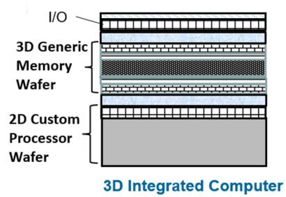
Or-Bach showed ideas for creating stacks of at least four devices using a combination of existing fab techniques he said were relatively low cost. He showed cutting out components with grinding processes and binding them face-to-face, using SiGe guide layers that are later etched away.

Zvi Or-Bach gave a high-level description of his proposed M3D techniques. (Image: MonolithIC 3D)
Existing bonders that can deliver alignment within 50nm tolerances were one element of his approach. He suggested his concepts could be used to build DRAMs that integrate memory and peripheral circuits in a single die.
Yang Du, a senior director at Qualcomm Research said M3D could be applied to a wide range of products. The technology could enable mating a memory array and an array of multiply-accumulate units to create an ideal neural network accelerator, an example shared by several speakers at the event.
In the short term, one of the top hurdles seems to be getting more EDA vendors involved in the work. A representative of Mentor Graphics showed the beginnings of efforts in parasitic extraction and verification for M3D structures. Qualcomm and ARM have worked with universities such as Georgia Tech on M3D design tools.

“There’s still a long way to go…We now have fine-grained 3D technology that looks very promising, and there are many challenges but they are not insurmountable,” said Mudit Bhargava, a representative of ARM Research.
CONTACT US
USA
Vilsion Technology Inc.
36S 18th AVE Suite A,Brington,Colorado 80601,
United States
E-mail:sales@vilsion.com
Europe
Memeler Strasse 30 Haan,D 42781Germany
E-mail:sales@vilsion.com
Middle Eastern
Zarchin 10St.Raanana,43662 Israel
Zarchin 10St.Raanana,43662 Israel
E-mail:peter@vilsion.com
African
65 Oude Kaap, Estates Cnr, Elm & Poplar Streets
Dowerglen,1609 South Africa
E-mail:amy@vilsion.com
Asian
583 Orchard Road, #19-01 Forum,Singapore,
238884 Singapore
238884 Singapore
E-mail:steven@vilsion.com
