FinFETs compete with FD-SOI
Intel has its own internal products already being designed for 22FL as well as hopes to attract foundry customers.
« Previously: Intel punts on transistor-density metric for 10nm
Intel will ramp its 22FFL node before the end of the year, clearly targeting the same kinds of chips for mobile and the Internet of Things as FD-SOI from Globalfoundries and others. A 0.5 PDK is ready now and will be in a version 1.0 by June.
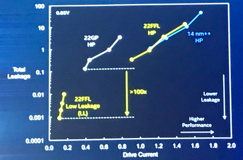
The process includes both high-performance transistors and low power ones with 100x less leakage than their peers in 28nm. It aims to compete with 28nm in costs by using simplified design rules and interconnects while using 14nm-like FinFETs.

Figure 1: Intel's 22FFL claims cost and power advantages over 28nm planar.
“We see it as the easiest-to-use FinFET process in the industry… think of this as FinFET for the masses,” said Stacy Smith, executive vice president of Intel’s fab and sales groups.
Specifically, the 22FFL process supports 45nm fin pitches, 108nm gate pitches, 90nm metal pitches using single patterning, 630nm logic cell heights, 18.8 million transistors/mm2 and 0.088µm2 SRAM bit cell. The gate and metal pitches are significantly relaxed from Intel’s first-generation FinFET 22nm node, which is at 90 and 80nm, respectively.
Mark Bohr, a senior fellow and director of process architecture and integration at Intel, showed leakage figures for 22FFL he claimed included sub-threshold, gate oxide and junction leakage. “All three matter,” he said, claiming the node has the “lowest leakage for any mainstream technology.”
Intel declined to provide a specific comparison between 22FL and 22nm FD-SOI. However, it has its own internal products already being designed for 22FL as well as hopes to attract foundry customers.
“Our roadmap going forward will be much, much broader in areas such as IoT and networking…and this enables us to get differentiated performance,” said Murthy Renduchintala, president of Intel’s client and IoT business and systems architecture group.
Globalfoundries' senior vice president of product management, Alain Mutricy, responded to the news of Intel's 22FFL. “Our process is fully qualified for production and we are seeing strong customer demand, with more than 50 active engagements in high-growth areas such as mobile, IoT and automotive,” Mutricy said.
In a blog, Mutricy noted both TSMC and Intel have now announced 22nm processes, two years after Globalfoundries announced its FD-SOI plans. The work “demonstrates the unprecedented innovation that is taking place at advanced nodes that are one or two steps off of the leading edge,” he wrote.
GF’s 22nm process is “fully qualified for production at our Fab 1 facility in Dresden, Germany,” he said. The company “plans to grow the overall [22nm] fab capacity [in Dresden] by 40% by 2020,” he added.
In addition, GF announced in February a joint venture fab to make 22nm FD-SOI products in China starting in 2019. It also tipped plans last year for a follow-on 12nm FD-SOI process in Dresden in 2019. “We expect others to follow our 12FDX lead,” he wrote.
For its part, the TSMC 22ULP node “will drive better RF components and it is very competitive in the low power IoT market,” said the TSMC spokeswoman.
More details on 14nm, foundry
Finally, Intel provided more details on its current 14nm process, now in its third variant, 14++. Intel has made three generations of x86 processors in the node as well as its Stratix 10 FPGAs. By the end of the year it will be making its LTE modems in the process, too.
Specifically, the Intel 14nm node uses 42nm Fin pitches, 52nm interconnect pitches, 70nm gate pitches, 399nm cell heights 399nm, 37.5 million transistors/mm2 and 0.050mm2 SRAM cell.
Intel’s use of self-aligned double patterning gives it advantages in tighter pitches at lower cost over other chip makers using litho-etch techniques, said Ruth Brain, a fellow and director of interconnect technology and integration at Intel.
Intel did not announce any new customers for its nascent foundry service. However it did win praise from IP and EDA leaders in a panel at the event led by its foundry executives.
Intel’s custom foundry group “has multiple repeat customers, and you never get that” if you can’t deliver products successfully, said Aart De Geus, chief executive of Synopsys.
The group is “now ready for prime time,” said Will Abbey, a senior vice president of sales and alliances at ARM, which has been working with Intel’s foundry for about 10 months.
keyword:sram
« Previously: Intel punts on transistor-density metric for 10nm
Intel will ramp its 22FFL node before the end of the year, clearly targeting the same kinds of chips for mobile and the Internet of Things as FD-SOI from Globalfoundries and others. A 0.5 PDK is ready now and will be in a version 1.0 by June.
The process includes both high-performance transistors and low power ones with 100x less leakage than their peers in 28nm. It aims to compete with 28nm in costs by using simplified design rules and interconnects while using 14nm-like FinFETs.

Figure 1: Intel's 22FFL claims cost and power advantages over 28nm planar.
“We see it as the easiest-to-use FinFET process in the industry… think of this as FinFET for the masses,” said Stacy Smith, executive vice president of Intel’s fab and sales groups.
Specifically, the 22FFL process supports 45nm fin pitches, 108nm gate pitches, 90nm metal pitches using single patterning, 630nm logic cell heights, 18.8 million transistors/mm2 and 0.088µm2 SRAM bit cell. The gate and metal pitches are significantly relaxed from Intel’s first-generation FinFET 22nm node, which is at 90 and 80nm, respectively.
Mark Bohr, a senior fellow and director of process architecture and integration at Intel, showed leakage figures for 22FFL he claimed included sub-threshold, gate oxide and junction leakage. “All three matter,” he said, claiming the node has the “lowest leakage for any mainstream technology.”
Intel declined to provide a specific comparison between 22FL and 22nm FD-SOI. However, it has its own internal products already being designed for 22FL as well as hopes to attract foundry customers.
“Our roadmap going forward will be much, much broader in areas such as IoT and networking…and this enables us to get differentiated performance,” said Murthy Renduchintala, president of Intel’s client and IoT business and systems architecture group.
Globalfoundries' senior vice president of product management, Alain Mutricy, responded to the news of Intel's 22FFL. “Our process is fully qualified for production and we are seeing strong customer demand, with more than 50 active engagements in high-growth areas such as mobile, IoT and automotive,” Mutricy said.
In a blog, Mutricy noted both TSMC and Intel have now announced 22nm processes, two years after Globalfoundries announced its FD-SOI plans. The work “demonstrates the unprecedented innovation that is taking place at advanced nodes that are one or two steps off of the leading edge,” he wrote.
GF’s 22nm process is “fully qualified for production at our Fab 1 facility in Dresden, Germany,” he said. The company “plans to grow the overall [22nm] fab capacity [in Dresden] by 40% by 2020,” he added.
In addition, GF announced in February a joint venture fab to make 22nm FD-SOI products in China starting in 2019. It also tipped plans last year for a follow-on 12nm FD-SOI process in Dresden in 2019. “We expect others to follow our 12FDX lead,” he wrote.
For its part, the TSMC 22ULP node “will drive better RF components and it is very competitive in the low power IoT market,” said the TSMC spokeswoman.
More details on 14nm, foundry
Finally, Intel provided more details on its current 14nm process, now in its third variant, 14++. Intel has made three generations of x86 processors in the node as well as its Stratix 10 FPGAs. By the end of the year it will be making its LTE modems in the process, too.
Specifically, the Intel 14nm node uses 42nm Fin pitches, 52nm interconnect pitches, 70nm gate pitches, 399nm cell heights 399nm, 37.5 million transistors/mm2 and 0.050mm2 SRAM cell.
Intel’s use of self-aligned double patterning gives it advantages in tighter pitches at lower cost over other chip makers using litho-etch techniques, said Ruth Brain, a fellow and director of interconnect technology and integration at Intel.
Intel did not announce any new customers for its nascent foundry service. However it did win praise from IP and EDA leaders in a panel at the event led by its foundry executives.
Intel’s custom foundry group “has multiple repeat customers, and you never get that” if you can’t deliver products successfully, said Aart De Geus, chief executive of Synopsys.
The group is “now ready for prime time,” said Will Abbey, a senior vice president of sales and alliances at ARM, which has been working with Intel’s foundry for about 10 months.
keyword:sram
CONTACT US
USA
Vilsion Technology Inc.
36S 18th AVE Suite A,Brington,Colorado 80601,
United States
E-mail:sales@vilsion.com
Europe
Memeler Strasse 30 Haan,D 42781Germany
E-mail:sales@vilsion.com
Middle Eastern
Zarchin 10St.Raanana,43662 Israel
Zarchin 10St.Raanana,43662 Israel
E-mail:peter@vilsion.com
African
65 Oude Kaap, Estates Cnr, Elm & Poplar Streets
Dowerglen,1609 South Africa
E-mail:amy@vilsion.com
Asian
583 Orchard Road, #19-01 Forum,Singapore,
238884 Singapore
238884 Singapore
E-mail:steven@vilsion.com
