Limitations of 3D NAND Scaling
The life span of 3D NAND might be a lot shorter than most people think.
At the Flash Memory Summit this year, Samsung announced its development of 1Tb 3D NAND, which would be used for commercial products launching next year. However, I wonder when the 4Tb 3D NAND will hit the market.
Based on the information available on TLC 512Gb 3D NAND with 64-layer on about 130mm2 die size (from Samsung and Toshiba) and assuming string stacking of 64-layer, I figured that in order to implement the 4Tb NAND chip:
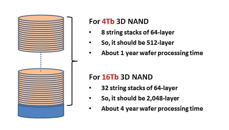
·Eight string stacks of 64-layer are needed. Which will make (512Gb x 8) = 4Gb
·The total layer then becomes 512-layer on 130mm2 die size
·It will take about a year to process a wafer, 5 weeks for memory logic plus 8 times (i.e. 8 string stack of 64-layer) 5 to 6 weeks for a 64-layer cell layer implementation. Therefore, the wafer processing time for a 512-layer will be about 45 to 53 weeks.

If this simple assessment is right, then it is practically impossible to implement the 4Tb NAND chip. If QLC is considered instead of TLC, there will be an improvement of 25 percent at best. So, a 410-layer will be needed for QLC 4Tb 3D NAND and about nine months of wafer processing time.
How about 16Tb 3D NAND? It needs 2,048-layers with four years of wafer processing time.
For the last several decades, NAND has achieved dazzling bit growth under Moore’s Law. When Moore’s Law ends and planar NAND switches to 3D NAND, many people expect 3D NAND will continuously expand its memory scaling in a vertical direction. However, 3D NAND just achieves price parity with planar NAND at 64-layer. Thus, 3D NAND will just start competing on price with planar NAND. And now I am thinking it will be practically impossible to expect 4Tb NAND.
The limitations of 3D NAND scaling seem obvious. Then, will 3D NAND reach the end of its life span? It might not be that far off.
At the Flash Memory Summit this year, Samsung announced its development of 1Tb 3D NAND, which would be used for commercial products launching next year. However, I wonder when the 4Tb 3D NAND will hit the market.
Based on the information available on TLC 512Gb 3D NAND with 64-layer on about 130mm2 die size (from Samsung and Toshiba) and assuming string stacking of 64-layer, I figured that in order to implement the 4Tb NAND chip:
·Eight string stacks of 64-layer are needed. Which will make (512Gb x 8) = 4Gb
·The total layer then becomes 512-layer on 130mm2 die size
·It will take about a year to process a wafer, 5 weeks for memory logic plus 8 times (i.e. 8 string stack of 64-layer) 5 to 6 weeks for a 64-layer cell layer implementation. Therefore, the wafer processing time for a 512-layer will be about 45 to 53 weeks.

If this simple assessment is right, then it is practically impossible to implement the 4Tb NAND chip. If QLC is considered instead of TLC, there will be an improvement of 25 percent at best. So, a 410-layer will be needed for QLC 4Tb 3D NAND and about nine months of wafer processing time.
How about 16Tb 3D NAND? It needs 2,048-layers with four years of wafer processing time.
For the last several decades, NAND has achieved dazzling bit growth under Moore’s Law. When Moore’s Law ends and planar NAND switches to 3D NAND, many people expect 3D NAND will continuously expand its memory scaling in a vertical direction. However, 3D NAND just achieves price parity with planar NAND at 64-layer. Thus, 3D NAND will just start competing on price with planar NAND. And now I am thinking it will be practically impossible to expect 4Tb NAND.
The limitations of 3D NAND scaling seem obvious. Then, will 3D NAND reach the end of its life span? It might not be that far off.
CONTACT US
USA
Vilsion Technology Inc.
36S 18th AVE Suite A,Brington,Colorado 80601,
United States
E-mail:sales@vilsion.com
Europe
Memeler Strasse 30 Haan,D 42781Germany
E-mail:sales@vilsion.com
Middle Eastern
Zarchin 10St.Raanana,43662 Israel
Zarchin 10St.Raanana,43662 Israel
E-mail:peter@vilsion.com
African
65 Oude Kaap, Estates Cnr, Elm & Poplar Streets
Dowerglen,1609 South Africa
E-mail:amy@vilsion.com
Asian
583 Orchard Road, #19-01 Forum,Singapore,
238884 Singapore
238884 Singapore
E-mail:steven@vilsion.com
