Is China ready for a memory chip fab?
With a lack of experienced engineers and equipment, will China’s decision to push into memory semiconductors be successful?
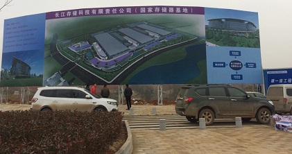
Figure 1: Signboard in XMC's memory fab construction site in Wuhan.
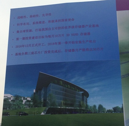
Figure 2: Memory fab's mission reads: "Gather global resources to build a centre for the world's memory chip industry-where China will control destiny."
Many China watchers believe that Tsinghua Unigroup’s plan to build a $30 billion memory chip in Nanjing was unexpected. This move is a head-scratcher, considering the uncertainty of China’s memory production even by a known entity as XMC in Wuhan. However, Tsinghua Unigroup’s Nanjing announcement speaks volumes for China’s determination to rule the global memory industry.
China is forging ahead despite a number of challenges. Among the biggest are a shortage of experienced memory chip engineers, a dearth of management expertise and growing scrutiny from the Committee on Foreign Investment in the United States (CFIUS).
In recent months, China’s proposed foreign investment deals were either blocked by or abandoned due to pressure from CIFUS. This sort of pushback makes it almost impossible for Chinese entities to buy foreign memory chip companies lock, stock and barrel.
Chinese media company Sina recently quoted Zhao Weiguo, chief executive of Tsinghua Unigroup, saying at a ceremony earlier this month:
In 2016, we started the construction of the memory base in Wuhan. This year we will build another two semiconductor manufacturing sites in Chengdu and Nanjing. The total investment of the three projects has exceeded $70 billion. Tsinghua Unigroup shoulders the future of IC Industry.
Tsinghua Unigroup’s stepped-up plans are palatable. Critics, however, point out that building a fab is one thing, but operating it is the hard part—especially when it comes to producing something as complex as 3D NAND flash.
Takashi Yunogami, a semiconductor engineer-turned consultant and an author of several books on the Japanese semiconductor industry, was a leading sceptic on the 3D NAND flash fab in Wuhan. However, he recently reversed his position. He told us this week that he has seen enough evidence from suppliers of materials and semiconductor manufacturing equipment to China.
Engineer shortage
Unfolding in China today, observed Yunogami, are battles over recruitment of engineering talent and semiconductor equipment (there is a shortage of some equipment designed to make NAND flash). Equally contentious are regional rivalries in China, with each city upping the ante to invite corporations to set up semiconductor fabs.
Before moving to further analysis of China’s memory production a whole, here’s a recap on who’s who among rising local memory chip vendors.
Brian Matas, vice president responsible for market research at IC insights, listed three key players, as of late last year:
XMC was purchased by Tsinghua Unigroup in July 2016 and set up a holding company called Yangtze River Storage Technology. It has broken ground for a new 300mm 3D NAND flash fab planned to come on-line in late 2017 or early 2018.
Sino King Technology plans to complete a DRAM fab in Hefei in late 2017.
Fujian Jin Hua Integrated Circuit intends a DRAM fab that will begin production in the third quarter, 2018.
Of these three, EE Times has learned that Sino King is, most likely, no longer in active operation.
The company, founded by Yukio Sakamoto, ex-Elpida CEO, tried to recruit 1,000 chip engineers from Japan, Taiwan and Korea, to remedy–head on–China’s shortage of experienced semiconductor engineers. Although Sino King managed to find 180 Japanese memory engineers willing to relocate, Sakamoto eventually met firm resistance from Chinese investors in Hefei, who refused to pay exorbitant salaries–as much as $887,000–to senior engineers.
Although Sino King’s salary promises exceeded normal practice in the semiconductor industry, Sakamoto’s action sheds light on China’s ongoing scramble to find the expertise necessary to get their fabs up and running.
During an interview with EE Times last month, one Silicon Valley chip executive stressed that it is not patents that China lacks, but “the manufacturing knowhow beyond patents.” This includes such mundane matters as entrance procedures to the building all the way to how to store wafers, he said. “These cannot be acquired; they must be learned.”
Yunogami agreed. According to sources supplying semiconductor equipment, XMC (now folded into YRST) has been insistent that suppliers bring to Wuan exactly the same equipment used by Samsung in its Xi’an fab, where the South Korean giant makes 32-layer NAND flash devices. [Samsung is making 64-layer vertical NAND memory in South Korea.]
Yunogami said, “XMC can buy equipment based on the same spec, but they can’t really run it unless they have people who know how to use it.”
There’s always a way around these problems, though. As the Silicon Valley executive quoted above told us, “China needs to learn from Korea.” That’s exactly what China is doing.
One of the first steps XMC took in its talent hunt was to poach almost 1,000 Chinese fab operators who have worked for Samsung in Xi’an. Further, XMC has been pursuing senior NAND engineers from Samsung and SK Hynix. XMC has also acquired a lot of internal technical information about Toshiba and Micron.
Yunogami has seen this movie before. Samsung used the same playbook when Korea was trying to catch up with Japan’s DRAM industry, he explained.
In the 1990s, Samsung heavily recruited Japanese DRAM engineers. These engineers kept their day jobs in Japan, but worked for Samsung, earning big money, on weekends. Weekend flights between Seoul and Tokyo were jammed with Japanese engineers.
Twenty years later, South Korea is getting similar treatment from China. Although Sino King’s strategy hasn’t exactly worked with Chinese investors, nobody can stop XMC in Wuan from poaching Samsung-trained engineers in Xi’an.
Learning progress
YRST, which now has XMC in its fold, has stated plans to build a 300mm fab for $24 billion. The first phase of construction began in late 2016 and the fab is expected to be completed in 2019.
Reports also say that YRST’s capacity is expected to be about 300,000 wafers monthly that will be used to produce 32-layer 3D NAND flash chips.

Figure 1: Signboard in XMC's memory fab construction site in Wuhan.
Yunogami believes YRST is making progress. By leveraging Spansion’s Mirror-Bit technology (originally developed for NOR, later picked up by Samsung to develop NAND), XMC carried out late last year its first and second test production of 32-layer 3D NAND flash. The yield in the first lot, tested in mid-November, “was zero” [as expected], said Yunogami. A second lot in December similarly produced no devices that can perform at full spec. But it’s suspected that there are some salvageable devices able to work at a lesser spec, Yunogami said.

Figure 2: Memory fab's mission reads: "Gather global resources to build a centre for the world's memory chip industry-where China will control destiny."
XMC appears to be following a normal learning curve in memory production.
Money talks
However, at a time when YRST in Wuhan is still in an early stage of NAND development, why is Tsinghua Unigroup in such a hurry for another memory fab in a different city?
This is a move unexpected even by some China experts.
Reached for comment, Dieter Ernst, an East-West Center senior fellow, took 24 hours to confirm that a memorandum of understanding has been signed between Tsinghua Unigroup and Nanjing. He explained, “According to the MoU, Tsinghua will invest $30 billion (funding source unknown) in Nanjing to build up to 300,000 wafers per month capacity of either DRAM or NAND. This is in addition to the 300,000 wafers per month by 2020 that it is building in Wuhan. Tsinghua also plans to spend $28 billion in Chengdu to build 500,000 wafers per month of advanced logic foundry capacity.”
But really, what’s going on? Isn’t this a bit reckless even for Tsinghua Unigroup?

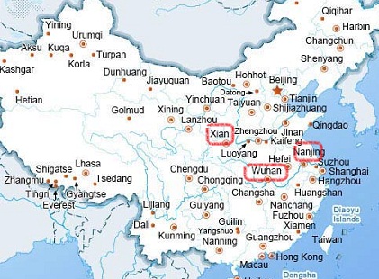
Figure 3: China’s memory triangle-Xi'an, Wuhan and Nanjing.
The Silicon Valley chip veteran we talked to acknowledged, “The stories and permutations [of various China fab moves] will likely give us headaches. But here is my perspective. To understand China, we have to follow the money.”
He said, “In China, the central government is the strategic passive money. It’s almost like a matching grant. Some oversight but pretty much uninvolved and un-participating in profits. There is one requirement, local government and private industry must provide more than 50% of funding.”
In other words, what appears to be a monolithic China led by the Communist Party is in fact a lot more fragmented, fraught with rivalries among local regional governments and cities all racing to succeed.
The U.S. executive suspects that “Tsinghua’s high-flying style and high pressure approach has not been all that successful in Wuhan. So Wuhan may be pulling back some.”
Meanwhile, it’s important to remember that TSMC, the world’s largest foundry, last March signed an agreement with the municipal government of Nanjing to finalise plans for its first 300mm wafer fab in China.
“TSMC did a head fake in Nanjing by talking about a fab, but not delivering (at least not fully) the scale Nanjing wants,” the U.S. executive speculated. “Not wanting to be out-classed by Wuhan as the next tier one city, I think Nanjing may have jumped in bed with Wuhan.”
As far as Tsinghua Unigroup’s announced fab in Nanjing is concerned, not everything is set in stone. They said that the fab will be manufacturing “either NAND or DRAM.”
High risk of overshooting
All these activities in China are inevitably inviting concerns about overcapacity.
Last year, IC Insights' Matas wrote, “Companies planning to significantly ramp up 3D NAND flash capacity include: Samsung, SK Hynix, Micron, Intel, Toshiba/SanDisk and XMC/Yangtze River Storage Technology and additional new Chinese producers possibly entering the market.”
Matas noted: “IC Insights believes that the future risk for overshooting 3D NAND flash market demand is very high and growing.”
Although Ernst is “a bit puzzled by the heroic assumptions” of people forecasting five years forward in a rapidly changing industry, he said, “Let’s assume that cumulative Chinese memory investments will indeed produce excess capacity in both DRAM and NAND.”
He asked rhetorically: “Shouldn’t we welcome this development, which might reduce the dependence on Samsung of our main downstream users?”
Ernst argued:
New memories are needed, but not many companies have the kind of money to invest in them. If there is no new entry, the industry will continue to be dominated by Samsung, a scenario disliked by all downstream users. If China comes to their rescue, why should we bother?
He added, “China’s decision to push into memory semiconductors may not be the best choice for China, because memory industry is a money burner. It costs billions of dollars in each generation of technologies, which often become ‘bleeding-edge technologies.’”
Ernst isn’t optimistic. He warned: “For China, this means decades of struggle and tons of money to be invested in high-risk projects with uncertain outcomes.”
If that’s the case, in his opinion, why bother?
CONTACT US
USA
Vilsion Technology Inc.
36S 18th AVE Suite A,Brington,Colorado 80601,
United States
E-mail:sales@vilsion.com
Europe
Memeler Strasse 30 Haan,D 42781Germany
E-mail:sales@vilsion.com
Middle Eastern
Zarchin 10St.Raanana,43662 Israel
Zarchin 10St.Raanana,43662 Israel
E-mail:peter@vilsion.com
African
65 Oude Kaap, Estates Cnr, Elm & Poplar Streets
Dowerglen,1609 South Africa
E-mail:amy@vilsion.com
Asian
583 Orchard Road, #19-01 Forum,Singapore,
238884 Singapore
238884 Singapore
E-mail:steven@vilsion.com
