Embedded MRAM moves into 22nm node
eMRAM has the ability to retain data through solder reflow at 260°C, and for more than 10 years at 125°C, plus read/write with outstanding endurance at 125°C.

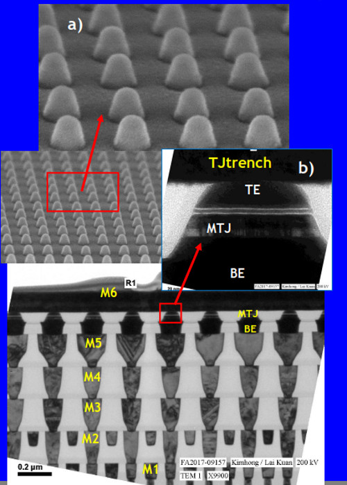
Figure 1: Globalfoundries' magnetic tunnel junction (MTJ) stack and integration was been optimized for a 400 degree Celsius, 60-minute post-MTJ patterning thermal budget and compatible with CMOS BEOL.
Among the foundries that have announced plans to put MRAM into production, one has outlined how it can improve data retention—significantly—for embedded applications.
At the recent 2017 International Symposium on VLSI Technology, Systems and Applications in Japan, Globalfoundries outlined in a technical paper Everspin Technologies' progress with moving embedded MRAM (eMRAM) forward into the 22nm process node.
In a telephone interview with* EE Times*, Dave Eggleston, Globalfoundries' vice president of embedded memory, said the key breakthrough highlighted in the paper is the ability for eMRAM to retain data through solder reflow at 260°C, and for more than 10 years at 125°C, plus read/write with outstanding endurance at 125°C. This will enable eMRAM to be used for general purpose MCUs and automotive SOCs, he said. “The thermal stability has not been there for the magnetic layers. If you solve that data retention problem then it opens up much wider markets," he added.
MRAM had demonstrated non-volatility, high reliability and manufacturability in previous technology nodes, Eggleston said, but has been challenged to scale to 2x nm node geometries and BEOL compatibility process temperatures for embedded memories. As outlined in the paper, the magnetic tunnel junction (MTJ) stack and integration was been optimised for a 400°C, 60-minute post-MTJ patterning thermal budget and compatible with CMOS BEOL.
The three major foundries are all introducing it as a product and customers are picking up Globalfoundries' PDK to started designing for it, said Eggleston. The major fab equipment makers started getting involved several years ago because they believed there was enough business, so the tools are available for deposition and etch of the MTJ. “They invested and developed products in conjunction with large fabs like us and with small companies such as Everspin," Eggleston said.
MCU customers, in the meantime, have started seriously looking at how MRAM can enhance their architectures, said Eggleston. “They get faster write speed and they get higher endurance," he said. This gives them the capability to use embedded MRAM where they might have previously used SRAM. Eggleston said the 2x nm node is the sweet spot in terms of circuitry simplicity and manufacturing costs.

Figure 1: Globalfoundries' magnetic tunnel junction (MTJ) stack and integration was been optimized for a 400 degree Celsius, 60-minute post-MTJ patterning thermal budget and compatible with CMOS BEOL.
The market opportunity for eMRAM is not dissimilar to those of other emerging memory technologies as well as incumbents: new high-volume markets include mobility, networking, data centers, Internet of Things (IoT) and automotive, said Eggleston. For Globalfoundries, the latter two are the most relevant. “We used to say they were largely the same, but as a foundry we got lots of traction in automotive," he said.
eFlash has been the incumbent embedded memory, but there are many emerging options that can potentially address these markets, said Eggleston. In addition to eMRAM, there is phase change memory (PCM), embedded Resistive RAM (eRRAM), carbon nanotube (CNT) and ferroelectric (FeFET). All have trade-offs when it comes to retention, efficiency and speed, he said. Both CNT and FeFET show promise, but are too immature, while PCM is too specialised and fading away from embedded applications.
“MRAM and RRAM both have similar capabilities," said Eggleston. “They're both backend aligned memories so that gives you the ability to pretty easily implement them into a logic process."
Processes include those that require bulk silicon, FD-SOI or FinFET. eFlash is built down into the silicon, he said, and would be more challenging to build into all of those variants.
RRAM is a simpler stack, said Eggleston, as there are fewer materials required between the electrodes. “It also doesn't require the same investment in equipment MRAM does," he said. "MRAM certainly requires unique capital equipment to do that complex stack." However, he said, RRAM hasn't shown the ability to provide the data retention, speed and endurance balance required by the broader market.
What MRAM offers over RRAM is versatility, said Eggleston, because its material composition can be tuned between electrodes. “You can tune it either for great data retention or for really fast write speed and endurance," he said. This tuneability, he added, will enable Globalfoundries to address the space at advanced nodes previously addressed by eFlash, as well as tune it for speed for use as a non-volatile cache in server processors and storage controllers.
CONTACT US
USA
Vilsion Technology Inc.
36S 18th AVE Suite A,Brington,Colorado 80601,
United States
E-mail:sales@vilsion.com
Europe
Memeler Strasse 30 Haan,D 42781Germany
E-mail:sales@vilsion.com
Middle Eastern
Zarchin 10St.Raanana,43662 Israel
Zarchin 10St.Raanana,43662 Israel
E-mail:peter@vilsion.com
African
65 Oude Kaap, Estates Cnr, Elm & Poplar Streets
Dowerglen,1609 South Africa
E-mail:amy@vilsion.com
Asian
583 Orchard Road, #19-01 Forum,Singapore,
238884 Singapore
238884 Singapore
E-mail:steven@vilsion.com
